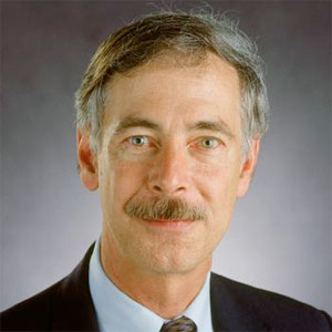
Biography
Current activities focus on improved transistors for use in rf and microwave systems; and on improved microwave circuit architectures, with emphasis on power amplifiers that are efficient and linear.
The device research activities cover the areas of GaAs- and InP-based HBTs; silicon on sapphire (SOS) CMOS devices; and GaN HFETs. We have developed GaAs-based HBTs with fmax values above 200GHz; GaInP/GaAs HBTs that suppress charge storage when they are operated in saturation; and novel packaging approaches that reduce thermal resistance by x2.5. We demonstrated microwave integrated circuits based on CMOS on SOS with low noise and high gain at 2.4GHz and above. We are currently focusing on HBTs with ultra-low knee voltages, for use in efficient amplifiers at low power supply voltage; on InP transistors with high gain in the mm-wave regime; and on GaN devices with breakdown voltages above 100V.
The circuit approaches being investigated include a novel power amplifier in which a dc-dc converter is incorporated in order to tailor the power supply voltage as a function of the instantaneous output power, avoiding clipping yet maximizing power efficiency. These amplifiers have already shown improvements of x1.4 over conventional circuits. Another thrust involves the use of switching mode amplifiers which are inherently highly efficient but suffer from poor linearity. Various techniques of efficiently linearizing these amplifiers are being developed.
Dr. Asbeck attended MIT, where he received his B.S. and Ph.D. degrees in 1969 and 1975, respectively, from the Electrical Engineering Department. He has worked at Sarnoff Research Center, Princeton, New Jersey, and at Philips Laboratory, Briarcliff Manor, New York, in the areas of quantum electronics and GaAlAs/GaAs laser physics and applications. In 1978, he joined Rockwell International Science Center, where he was involved in the development of high speed devices and circuits based on III-V compounds and heterojunctions. He investigated the influence of GaAs substrates on the behavior of field-effect transistors. More recently, he participated in the effort to develop heterojunction bipolar transistors based on GaAlAs/GaAs and InAlAs/InGaAs materials systems, and has contributed widely in the areas of physics, fabrication and applications of these devices. In 1989 he became the Principal Scientist of the High Speed Electronics and Optoelectronics Function at Rockwell International Science Center. In 1991, Dr. Asbeck joined the University of California, San Diego as Professor in the Department of Electrical and Computer Engineering. His research interests are in development of high speed heterojunction transistors and optoelectronic devices.
Dr. Asbeck's research has led to more than 120 publications. He has served on technical program committees of IEDM, DRC, MMMIC, GaAs IC Symposium, and Symposium on GaAs and Related Compounds. He was Rockwell Engineer of the Year in 1986. He is the General Chairman of the 1996 DRC.
https://qi.ucsd.edu/powering-6g/https://qi.ucsd.edu/powering-6g/